AOI machine programming methodAuthor : Adrian September 17,solder paste screen 2025Table of ContentsIn the fast-paced world of PCB manufacturing, ensuring quality and precision is critical. One of the most effective ways to achieve this is through Automated Optical Inspection (AOI) systems. But how do you program an AOI machine to deliver accurate results? In this guide, we’ll dive into the AOI machine programming method, exploring the use of an AOI automated teaching tool, the process for AOI code, and the steps for generating inspection instructions. Whether you’re new to AOI or looking to optimize your setup, this blog offers practical insights to enhance your inspection process.
What Is AOI Machine Programming and Why Does It Matter?AOI machine programming is the process of setting up an Automated Optical Inspection system to detect defects on printed circuit boards (PCBs) during manufacturing. This involves creating a set of instructions or code that tells the machine what to look for—such as missing components, solder defects, or misalignments—and how to interpret the data it captures. With the right programming, an AOI system can save time, reduce costs, and ensure high-quality output by catching errors early in the production line. The importance of effective programming cannot be overstated. Poorly programmed AOI machines may miss critical defects or generate false positives, leading to wasted resources and potential failures in the final product. By mastering AOI programming, manufacturers can achieve consistent results, improve efficiency, and maintain customer satisfaction.
Key Components of AOI Machine ProgrammingBefore diving into the programming methods, let’s break down the essential components that form the foundation of an AOI system’s operation. Understanding these elements will help in crafting effective inspection instructions.
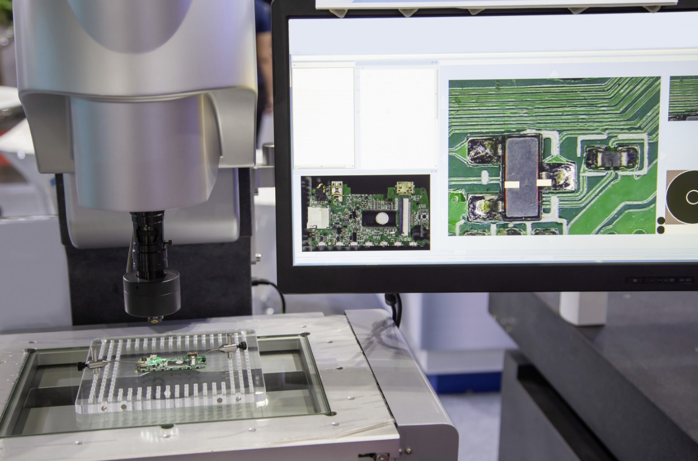
Step-by-Step AOI Machine Programming MethodProgramming an AOI machine is a structured process that requires attention to detail. Below, we outline a practical method to ensure accurate and efficient inspections, incorporating the use of automated teaching tools and code generation. Step 1: Prepare the Reference DataThe first step in AOI programming is to establish a baseline for comparison. This is often done using a “golden board”—a defect-free PCB that serves as the standard—or by importing CAD (Computer-Aided Design) data. The reference data tells the AOI system what a perfect board looks like, including component placement, solder joints, and other features. Ensure that the reference data is accurate and up-to-date. For example, if your PCB design has components with a placement tolerance of ±0.1 mm, this value must be reflected in the programming to avoid false defect calls.
Step 2: Use an AOI Automated Teaching ToolAn AOI automated teaching toolsimplifies the programming process by guiding users through setup with minimal manual input. These tools often come integrated into the AOI software and use machine learning or predefined templates to teach the system what to inspect. For instance, the teaching tool might automatically detect component outlines and solder joint patterns on a sample PCB. It then generates initial inspection parameters, such as brightness thresholds or defect size limits (e.g., detecting solder bridges larger than 0.05 mm). Users can fine-tune these settings to match specific requirements, saving significant time compared to manual programming. Automated teaching tools are especially useful for complex boards with hundreds of components, as they reduce human error and ensure consistency across multiple production runs. Step 3: Define Inspection Parameters and Defect CriteriaOnce the reference data is loaded and the teaching tool has provided a starting point, it’s time to set specific inspection parameters. This includes defining what constitutes a defect and setting thresholds for acceptable variations. For example:
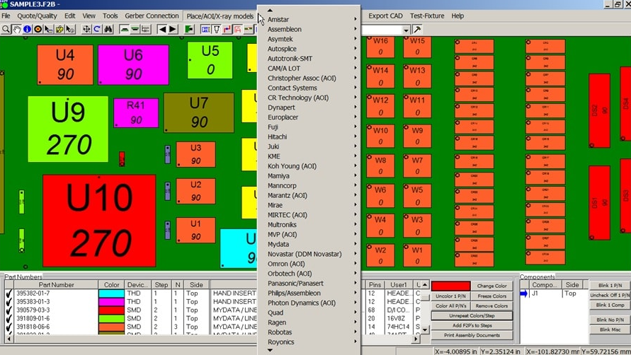
These parameters must align with industry standards like IPC-A-610, which defines acceptability criteria for electronic assemblies, ensuring your AOI system delivers reliable results. Step 4: Develop the Process for AOI CodeThe process for AOI codeinvolves translating the defined parameters into a format the machine can execute. This code acts as a set of instructions for the AOI system, guiding how it captures images, processes data, and identifies defects. Modern AOI systems often use graphical interfaces where users input parameters through dropdowns or sliders, automatically generating the underlying code. However, for advanced customization, some systems allow direct scripting using languages like Python or proprietary formats. The code specifies details such as:
Testing the code on a small batch of boards is crucial to ensure it performs as expected before full-scale deployment.
Step 5: Generate Inspection InstructionsThe final step is generating inspection instructionsthat the AOI machine follows during operation. These instructions are essentially the compiled output of your programming efforts, combining reference data, parameters, and code into a cohesive workflow. Inspection instructions detail the sequence of actions, such as:
Once generated, these instructions are saved as a “recipe” or program file in the AOI system, ready to be reused for identical board designs.
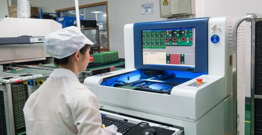
Best Practices for Optimizing AOI ProgrammingTo get the most out of your AOI machine programming, consider these best practices that enhance accuracy and efficiency. Regularly Update Reference DataPCB designs evolve, and so should your reference data. If a component supplier changes a part’s dimensions by even 0.05 mm, update the golden board or CAD file to reflect this. Failing to do so can lead to false positives or missed defects. Minimize False AlarmsFalse alarms slow down production as operators must manually verify flagged issues. Fine-tune defect thresholds and use automated teaching tools to train the system on real-world variations, reducing unnecessary alerts by up to 30% in some cases. Integrate with Production LinesProgram your AOI system to communicate with other equipment, like pick-and-place machines or reflow ovens. For instance, if the AOI detects a recurring defect at a specific solder joint, it can send feedback to adjust the upstream soldering temperature by 5°C to prevent future issues. Test and ValidateAfter programming, run the AOI system on a test batch of 50-100 boards. Analyze the defect detection rate and false positive rate. Aim for a detection accuracy of at least 95% before scaling up to full production.
Benefits of Mastering AOI Machine ProgrammingInvesting time in effective AOI programming yields significant advantages for PCB manufacturers:
Challenges in AOI Programming and How to Overcome ThemWhile AOI programming offers many benefits, it comes with challenges. Here are common issues and solutions:
Conclusion: Elevate Your PCB Inspection with AOI ProgrammingMastering the AOI machine programming methodis a game-changer for PCB manufacturing. By utilizing an AOI automated teaching tool, following a streamlined process for AOI code, and carefully generating inspection instructions, manufacturers can achieve unparalleled precision and efficiency. The steps outlined—preparing reference data, setting parameters, coding, and testing—provide a clear path to success. At ALLPCB, we’re committed to supporting your journey in PCB production with cutting-edge solutions and expert guidance. Implement these programming techniques to enhance your AOI system’s performance and deliver top-quality boards every time. Share · · · ·  The Role of Flux in PCB Wave Soldering: Selection, Application, and Residue RemovalMarch 16, 2026PCB wave soldering flux types include rosin, water-soluble, and no-clean options with varying activity levels for oxide removal and solder flow. This guide covers selection criteria, spray foam drop-jet application methods, residue removal processes, and alternatives like nitrogen blanketing to boost joint reliability and yields for engineers. Article Achieving Uniform Solder Fillets in PCB Wave Soldering: Process ControlMarch 16, 2026Achieve uniform solder fillets in PCB wave soldering with process control strategies. Optimize flux, preheat, wave height, conveyor speed for consistent fillet shape, height, and wetting balance. Includes visual inspection tips and troubleshooting for reliable through-hole assemblies. Boost quality in production. Article Optimizing Conveyor Speed for Efficient PCB Wave SolderingMarch 16, 2026Learn PCB wave soldering conveyor speed calculation to manage dwell time, immersion depth, and throughput effectively. Electric engineers get practical steps, best practices, and troubleshooting tips for higher process efficiency and fewer defects in wave soldering operations. Article Understanding IPC Standards for PCB Surface Finishes: Ensuring Quality and ComplianceMarch 11, 2026Understand IPC standards IPC 4552 ENIG and IPC 4553 immersion silver for PCB surface finishes. Ensure compliance, enhance solderability, and prevent common defects to achieve reliable, high quality circuit boards. Article Miniaturization Challenges in PCB AssemblyMarch 11, 2026Navigate the complexities of high density interconnect PCB assembly and precise component placement. Learn to tackle miniaturization challenges, from tiny part handling to thermal stress, ensuring robust and reliable electronics. Article High Speed Routing Techniques: PCBMarch 11, 2026Master high speed routing in PCBs to ensure signal integrity and minimize electromagnetic interference. Learn essential techniques for robust designs, from controlled impedance to differential pair strategies. Prevent performance issues and achieve reliable electronics. ArticleGet Instant PCB |